Smart Connectivity
The drive toward miniaturization in the electronics industry has been particularly rapid over the past two decades. Many applications and products, for instance in the ever-growing field of semiconductor applications, could only be realized due to new fabrication and bonding techniques. Here, laser technology will continue to drive forward technological advancements.
Typical Laser Applications
-
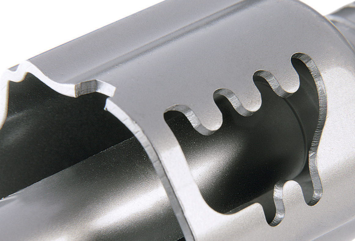
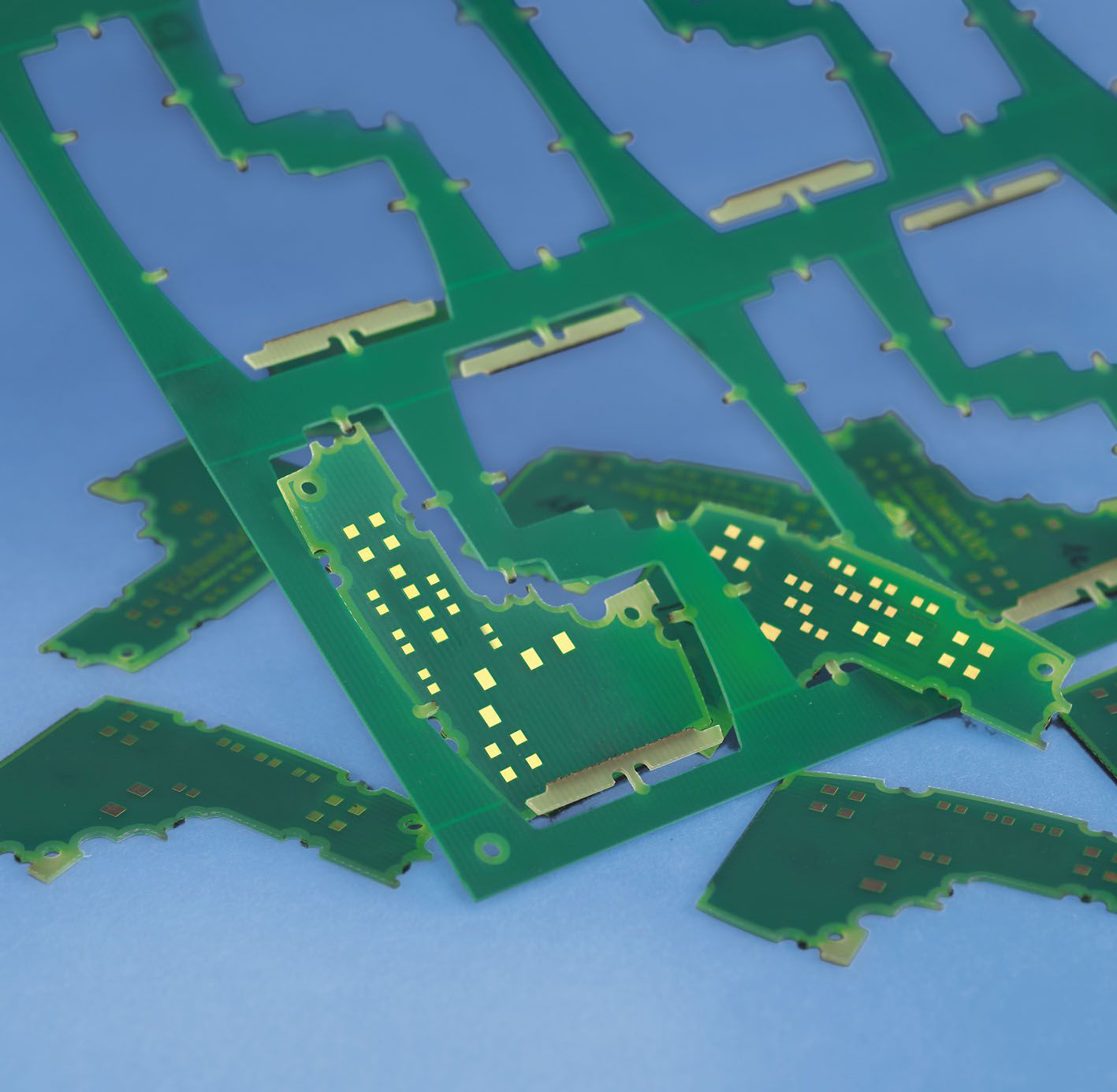
Laser cutting of glass, ceramics and plastics, e.g. for housings and other components with no-post-processing of cut edges
-
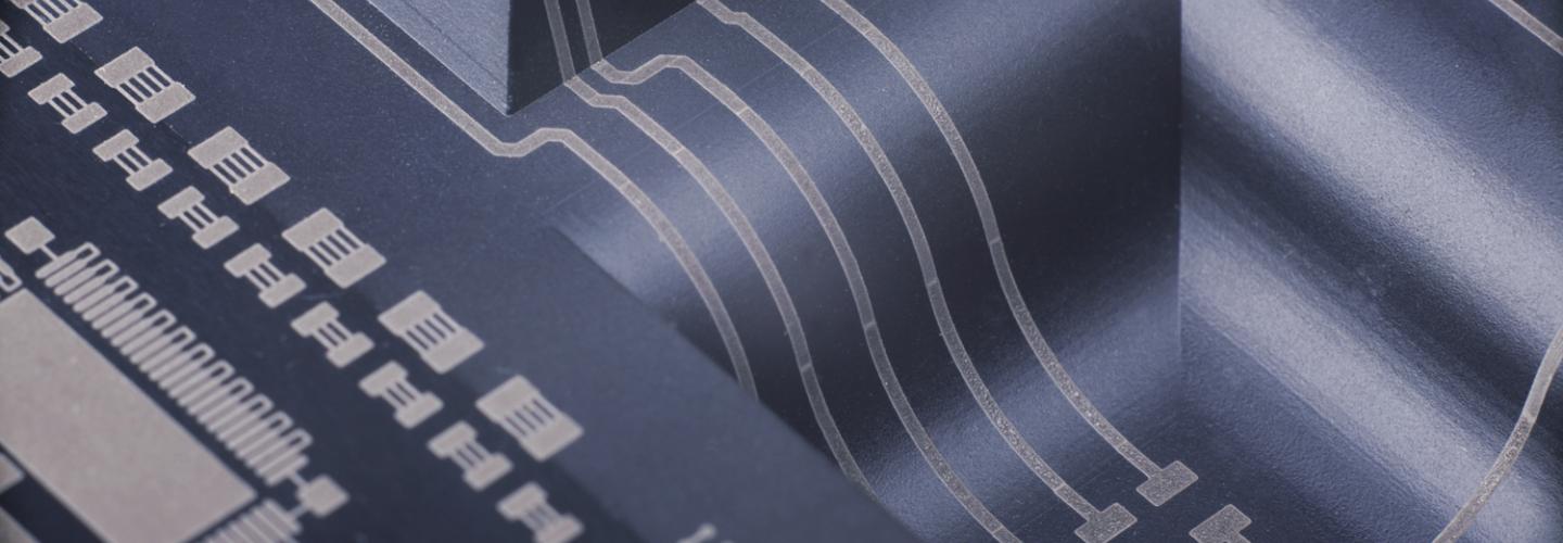
Laser microstructuring of semiconductors, glass, displays and other electronic components
-
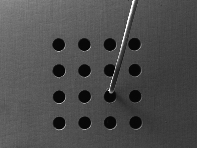
Laser microdrilling (microvias) of electronic components , e.g. HDI (high density interconnect) circuit boards
-
Laser direct structuring e.g. laser pre-treatment of plastic injection molded parts for generating integrated electrical connections and switches for 3D MIDs (molded interconnected devices)
-
Laser soldering for selective soldering of electronic components
-
Laser marking for environmentally friendly and durable marking of cables, electronic components, PCBs, wafers and numerous other component types and materials
-
Laser trimming (laser compensation) of resistors and capacitors
Lasers as Tools
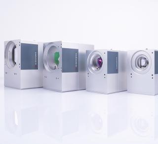
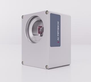
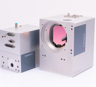
By transforming lasers into universal tools, scanning solutions help to add functionality and value to materials. SCANLAB's broad palette of scanning solutions fulfills demands for higher speed, more precision, greater efficiency or improved environmental compatibility.

